| CPC H01L 23/3171 (2013.01) [H01L 23/3135 (2013.01); H01L 24/13 (2013.01); H01L 24/14 (2013.01); H01L 24/16 (2013.01); H01L 24/73 (2013.01); H01L 25/0657 (2013.01); H01L 25/18 (2013.01); H01L 22/12 (2013.01); H01L 2224/0401 (2013.01); H01L 2224/05073 (2013.01); H01L 2224/05166 (2013.01); H01L 2224/05573 (2013.01); H01L 2224/05647 (2013.01); H01L 2224/10125 (2013.01); H01L 2224/13016 (2013.01); H01L 2224/1357 (2013.01); H01L 2224/13147 (2013.01); H01L 2224/13564 (2013.01); H01L 2224/13583 (2013.01); H01L 2224/13611 (2013.01); H01L 2224/13639 (2013.01); H01L 2224/13647 (2013.01); H01L 2224/13655 (2013.01); H01L 2224/13657 (2013.01); H01L 2224/14515 (2013.01); H01L 2224/16227 (2013.01); H01L 2224/73204 (2013.01); H01L 2225/06513 (2013.01); H01L 2225/06517 (2013.01); H01L 2924/1436 (2013.01)] | 20 Claims |
|
1. A semiconductor package comprising:
a base;
a first chip on the base; and
first connection patterns that connect and couple the base and the first chip,
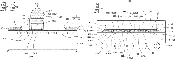
wherein the first chip includes a substrate, pad patterns on the substrate, a passivation layer on the substrate and having openings, and pillars on the substrate,
wherein the pad patterns include a first signal pad and a second signal pad,
wherein the first connection patterns are in contact with the pillars,
wherein the pillars include a first signal pillar in contact with the first signal pad and a second signal pillar in contact with the second signal pad,
wherein the openings in the passivation layer include a first opening having a sidewall facing a side surface of the first signal pillar and surrounding the side surface of the first signal pillar, and a second opening having a sidewall facing a side surface of the second signal pillar and surrounding the side surface of the second signal pillar, and
wherein a maximum width of the second opening is greater than a maximum width of the first opening.
|