| CPC H01L 23/3135 (2013.01) [H01L 23/4012 (2013.01); H01L 23/5383 (2013.01)] | 20 Claims |
|
1. A semiconductor package, comprising:
a circuit board structure, comprising:
a core layer and first and second build-up layers respectively located on two surfaces of the core layer;
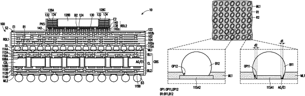
first conductive patterns comprising inner conductive patterns and outer conductive patterns surrounding the inner conductive patterns, located on the first build-up layer; and
a first mask layer adjacent to the outer conductive patterns and the inner conductive patterns and in contact with the first build-up layer;
a first redistribution layer structure, disposed over the circuit board structure; and
first bonding elements comprising outer bonding elements and inner bonding elements, disposed between and electrically connected to the first redistribution layer structure and the circuit board structure, wherein the outer bonding elements completely cover top surfaces and sidewalls of the outer conductive patterns, and the inner bonding elements partially cover top surfaces of the inner conductive patterns, and
wherein a portion of an encapsulation layer is disposed between the first redistribution layer structure and the circuit board structure and another portion of the encapsulation layer covers a sidewall of the circuit board structure, and
wherein a sidewall of the redistribution layer structure is flushed with a sidewall of the encapsulation layer.
|