| CPC H01L 22/32 (2013.01) [G11C 29/1201 (2013.01); H01L 2224/16145 (2013.01); H01L 2224/16225 (2013.01); H01L 2224/48091 (2013.01); H01L 2224/48227 (2013.01); H01L 2924/15311 (2013.01); H01L 2924/181 (2013.01)] | 20 Claims |
|
1. A semiconductor chip, comprising:
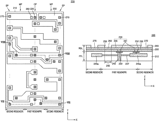
a plurality of chip pads disposed in a first region of a chip body, the plurality of chip pads being spaced apart in a first direction and in a second direction, which is substantially opposite to the first direction in a plan view;
a redistribution wiring test pad disposed in the first region of the chip body, spaced apart from the plurality of chip pads;
a redistribution wiring connection pad disposed in a second region of the chip body;
a redistribution wiring layer electrically connected to the plurality of chip pads, wherein the plurality of chip pads, the redistribution wiring test pad and the redistribution wiring connection pad are sequentially connected to the same redistribution wiring layer in the first direction in the plan view; and
an internal circuit element including a memory cell array, wherein the internal circuit element is not vertically overlapped by a lower portion of the redistribution wiring test pad in the first region of the chip body,
wherein the redistribution wiring test pad is positioned at a different height from the plurality of chip pads in a direction perpendicular to a plane of the semiconductor chip.
|
|
9. A semiconductor chip, comprising:
a chip body having at least two chip pads thereon;
at least one redistribution wiring test pad in a first region of the chip body, each of the at least one redistribution wiring test pad being spaced apart from each of the at least two chip pads in a plan view;
at least one redistribution wiring connection pad in a second region of the chip body, the second region being different from the first region, each redistribution wiring connection pad being spaced apart from each of the at least two chip pads in the plan view;
at least one redistribution wiring structure, each of the at least one redistribution wiring structure electrically connected to each of the at least two chip pads, wherein a redistribution wiring test pad of the at least one redistribution wiring test pad corresponding to one of the at least two chip pads and the redistribution wiring connection pad corresponding to the other of the at least two chip pads are directly connected to the same redistribution wiring structure; and
a memory cell array, wherein the memory cell array is not vertically overlapped by a lower portion of the at least one redistribution wiring test pad in the first region of the chip body;
wherein the at least one redistribution wiring structure includes a redistribution wiring layer, and the redistribution wiring layer extends on the chip body in a first direction from each of the at least two chip pads to an edge portion of the chip body,
the at least one redistribution wiring test pad is disposed between each of the at least two chip pads and the at least one redistribution wiring connection pad in the first direction, the redistribution wiring layer is a single continuous metal layer, and
the at least one redistribution wiring test pad is positioned at a different height from the at least two chip pads in a direction perpendicular to a plane of the semiconductor chip.
|
|
16. A semiconductor chip, comprising:
a package board;
a chip body on the package board, the chip body having at least two chip pads thereon;
at least one redistribution wiring test pad in a first region of the chip body, each of the at least one redistribution wiring test pad being spaced apart from each of the at least two chip pads in a plan view;
at least one redistribution wiring connection pad in a second region of the chip body, the second region being different from the first region, each redistribution wiring connection pad being spaced apart from each of the at least two chip pads in the plan view;
at least one redistribution wiring structure, each of the at least one redistribution wiring structure electrically connected to each of the at least two chip pads, wherein a redistribution wiring test pad of the at least one redistribution wiring test pad corresponding to one of the at least two chip pads and the redistribution wiring connection pad corresponding to the other of the at least two chip pads are directly connected to the same redistribution wiring structure;
a memory cell array, wherein the memory cell array is not vertically overlapped by a lower portion of the at least one redistribution wiring test pad in the first region of the chip body; and
a bonding wire that electrically connects the at least one redistribution wiring connection pad to the package board,
wherein the at least one redistribution wiring structure includes a redistribution wiring layer, and the redistribution wiring layer extends on the chip body in a first direction from each of the at least two chip pads to an edge portion of the chip body, and
the at least one redistribution wiring test pad is disposed between each of the at least two chip pads and the at least one redistribution wiring connection pad in the first direction, the redistribution wiring layer is a single continuous metal layer.
|