| CPC H01L 22/26 (2013.01) [H01J 37/32449 (2013.01); H01J 37/32513 (2013.01); H01J 37/32935 (2013.01); H01L 21/31116 (2013.01); H01L 21/31144 (2013.01); H01J 2237/334 (2013.01)] | 20 Claims |
|
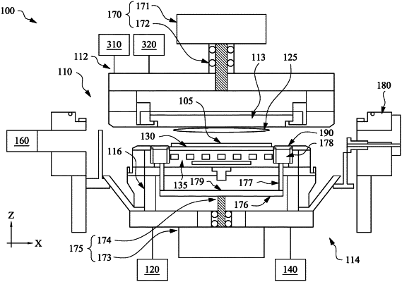
1. A method, comprising:
forming an inner chamber in a process chamber of a plasma processing apparatus, the inner chamber having smaller volume than the process chamber;
introducing at least one gas into the inner chamber;
measuring flow of the at least one gas into the inner chamber;
adjusting the flow of the at least one gas to a desired rate; and
processing a wafer by the at least one gas at the desired rate while the inner chamber is not formed.
|