| CPC H01L 21/823807 (2013.01) [H01L 21/02532 (2013.01); H01L 21/02609 (2013.01); H01L 21/3065 (2013.01); H01L 21/823821 (2013.01); H01L 21/823878 (2013.01); H01L 21/823892 (2013.01); H01L 27/0924 (2013.01); H01L 27/0928 (2013.01); H01L 29/045 (2013.01); H01L 29/0653 (2013.01); H01L 29/1054 (2013.01); H01L 29/1083 (2013.01); H01L 29/161 (2013.01)] | 20 Claims |
|
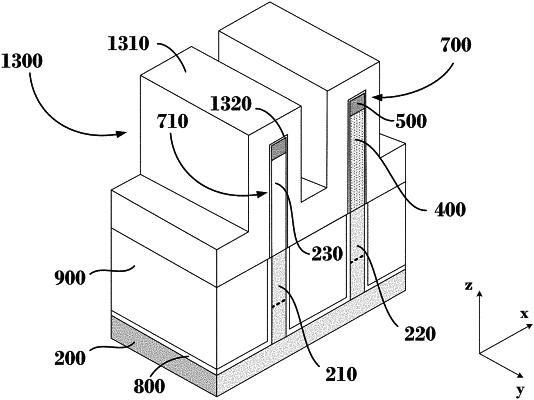
1. A semiconductor structure, comprising:
a semiconductor substrate;
a first fin structure comprising:
a first epitaxial layer disposed on the semiconductor substrate; and
a second epitaxial layer, thinner than the first epitaxial layer, in contact with and covering an entire top surface of the first epitaxial layer;
a first gate dielectric layer in contact with the first and second epitaxial layers;
a second fin structure comprising:
a third epitaxial layer, different from the first epitaxial layer, disposed on the semiconductor substrate; and
a fourth epitaxial layer, thinner than the third epitaxial layer, in contact with and covering an entire top surface of the third epitaxial layer;
a second gate dielectric layer in contact with the third and fourth epitaxial layers; and
an isolation region between the first and second fin structures, wherein a top surface of the isolation region and bottom surfaces of the first and third epitaxial layers are on a same surface plane.
|