| CPC H01L 21/76894 (2013.01) [H01L 21/02013 (2013.01); H01L 24/94 (2013.01)] | 4 Claims |
|
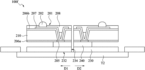
1. A manufacturing method of a chip package, comprising:
attaching a side of a package structure to a first adhesive tape, wherein the package structure is a wafer level package structure to be cut into a plurality of chip packages that each comprises a chip, the package structure has a carrier facing away from the side and a wafer between the carrier and the first adhesive tape, and the carrier has a top surface which is a plane;
cutting the package structure from the top surface of the carrier with a modified laser such that the package structure is cut from a top surface of the package structure to a bottom surface of the package structure;
attaching a second adhesive tape to the top surface of the carrier;
removing the first adhesive tape; and
expanding the second adhesive tape to divide the package structure into a plurality of chip packages, wherein each of the chip packages has a continuous sidewall that is flat and extends from a top surface of one of the chip packages to a bottom surface of said one of the chip packages.
|