| CPC H01L 21/76825 (2013.01) [H01L 21/486 (2013.01); H01L 21/76877 (2013.01)] | 14 Claims |
|
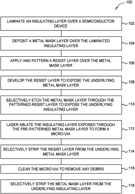
1. A method of forming a micro-via structure in a semiconductor device, comprising:
laminating a polymeric material layer over a conductive layer on the semiconductor device, wherein the semiconductor device comprises:
a substrate;
an insulating layer atop the substrate; and
the conductive layer atop the insulating layer;
depositing a metal mask layer over the polymeric material layer;
applying, patterning, and developing a resist layer over the metal mask layer, wherein developing the resist layer forms a trench in the resist layer corresponding to a desired lateral dimension of the micro-via structure;
etching the metal mask layer through the trench in the developed resist layer, wherein etching the metal mask layer extends the trench into the metal mask layer and exposes a portion of the polymeric material layer; and
laser ablating the exposed portion of the polymeric material layer using an ultraviolet (UV) laser in a pulse-burst mode and the pulse burst mode provides pulses at frequency of 50 MHz or more and an energy between 5 nJ and 10 nJ, wherein laser ablating the exposed portion of the polymeric material layer forms the micro-via structure therein having the desired lateral dimension and exposes the conductive layer.
|