| CPC H01L 21/7682 (2013.01) [H01L 21/76837 (2013.01); H01L 21/76877 (2013.01); H01L 23/528 (2013.01); H01L 23/5329 (2013.01); H10B 12/315 (2023.02); H10B 12/482 (2023.02); H10B 12/485 (2023.02); H10B 12/34 (2023.02)] | 7 Claims |
|
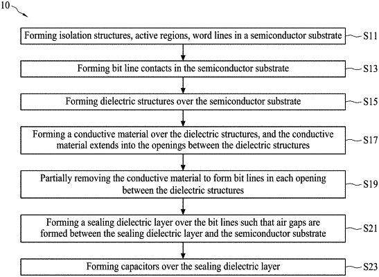
1. A method for preparing a semiconductor device, comprising:
forming a first dielectric structure and a second dielectric structure over a semiconductor substrate;
forming a conductive material over the first dielectric structure and the second dielectric structure, wherein the conductive material extends into a first opening between the first dielectric structure and the second dielectric structure;
partially removing the conductive material to form a first bit line and a second bit line in the first opening; and
forming a sealing dielectric layer over the first bit line and the second bit line such that an air gap is formed between the sealing dielectric layer and the semiconductor substrate,
wherein a top surface of the semiconductor substrate between the first bit line and the second bit line is exposed after the partial removal of the conductive material.
|