| CPC H01L 21/76224 (2013.01) [H01L 27/1463 (2013.01); H01L 27/1464 (2013.01); H01L 27/14643 (2013.01); H01L 27/14685 (2013.01)] | 20 Claims |
|
1. A method for forming an image sensor, the method comprising:
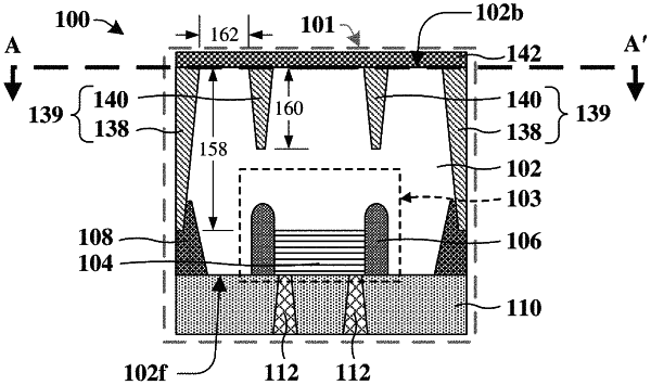
forming a pixel on a first side of a substrate, wherein the pixel comprises a photodetector in the substrate, and wherein the photodetector comprises a guard ring extending into the first side of the substrate;
forming an interconnect structure electrically coupled to the pixel on the first side of the substrate;
patterning a second side of the substrate, opposite the first side of the substrate, to form an outer isolation opening and an inner isolation opening, wherein the outer isolation opening extends into the substrate to a first depth and laterally surrounds the pixel along a boundary of the pixel, wherein the inner isolation opening extends into the substrate to a second depth, less than the first depth, and overlies the photodetector, and wherein the inner isolation opening has a ring-shaped top layout; and
depositing a first dielectric layer in the outer isolation opening and the inner isolation opening to form a dual trench isolation structure.
|