| CPC H01L 21/563 (2013.01) [H01L 21/78 (2013.01); H01L 23/31 (2013.01); H01L 23/5384 (2013.01); H01L 23/5386 (2013.01)] | 20 Claims |
|
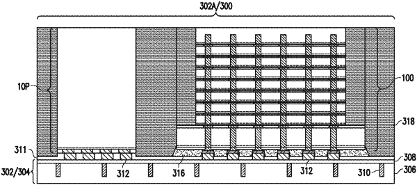
1. A method comprising:
attaching a logic die to a top side of an interposer, the interposer comprising a first die connector and a second die connector on the top side of the interposer and a first dielectric layer covering at least one sidewall of the first die connector and at least one sidewall of the second die connector, the logic die being coupled to the first die connector and to the first dielectric layer, the second die connector being exposed by the logic die;
recessing the first dielectric layer, the recessing exposing at least one sidewall of the second die connector; and
attaching a memory device to the top side of the interposer, the memory device being coupled to the second die connector.
|