| CPC H01L 21/0275 (2013.01) [H01L 21/0228 (2013.01); H01L 21/02362 (2013.01)] | 20 Claims |
|
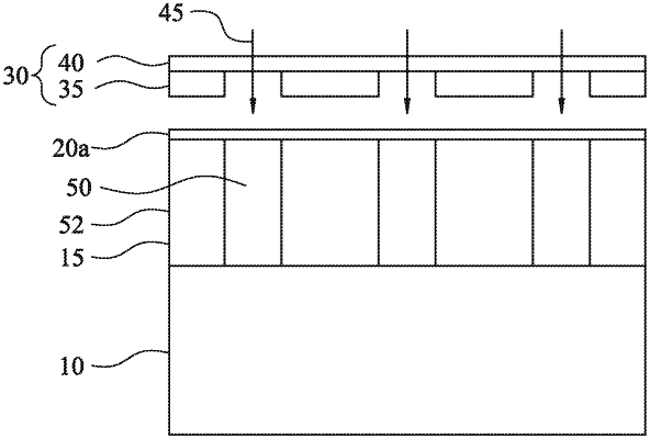
1. A method of forming a pattern in a photoresist layer,
comprising:
forming a photoresist layer over a substrate,
wherein the photoresist layer comprises a metal-containing photoresist composition;
reducing moisture or oxygen absorption characteristics of the photoresist layer,
wherein the reducing moisture or oxygen absorption characteristics of the photoresist layer comprises performing a surface treatment to a surface of the photoresist layer, wherein the surface treatment comprises changing the surface of the photoresist layer from a hydrophilic surface to a hydrophobic surface;
selectively exposing the photoresist layer to actinic radiation to form a latent pattern; and
developing the latent pattern by applying a developer to the selectively exposed photoresist layer to form a pattern.
|