| CPC H01L 21/02359 (2013.01) [H01L 21/76251 (2013.01); H01L 21/84 (2013.01); H01L 27/1203 (2013.01); H01L 29/0649 (2013.01)] | 20 Claims |
|
1. A semiconductor-on-insulator (SOI) substrate comprising:
a handle substrate;
a device layer overlying a central portion of the handle substrate, but not overlying a peripheral region of the handle substrate; and
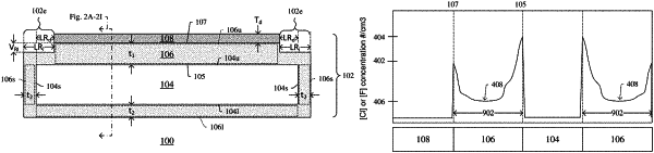
an insulator layer separating the handle substrate from the device layer, the insulator layer meeting the device layer at a first interface and meeting the handle substrate at a second interface, wherein the insulator layer comprises a getter material having a getter concentration profile;
wherein the handle substrate contains getter material and has a handle getter concentration profile, the handle getter concentration profile having a peak at the second interface and a gradual decline beneath the second interface until reaching a handle getter concentrations;
wherein the insulator layer includes a central insulator region that is directly between the central portion of the handle substrate and the device layer, and includes a peripheral insulator region that is directly over the peripheral region of the handle substrate, wherein the central insulator region has a central region thickness as measured perpendicular from the first interface to the second interface and wherein the peripheral insulator region has a peripheral region thickness as measured perpendicular from an upper surface of the handle substrate to an upper surface of the peripheral insulator region, the central region thickness being greater than the peripheral region thickness.
|