| CPC G11C 13/047 (2013.01) [H10B 63/30 (2023.02); H10N 70/011 (2023.02); H10N 70/257 (2023.02); H10N 70/8825 (2023.02); H10N 70/8828 (2023.02); H10N 70/8833 (2023.02)] | 17 Claims |
|
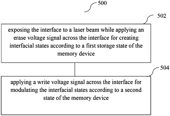
1. A method of switching between first and second states of a van der Waals heterostructure, vdWH, memory device comprising a first two-dimensional, 2D, material and a second 2D material with an interface therebetween, the method comprising the steps of:
exposing the interface to a laser beam while applying an erase voltage signal across the interface for creating interfacial states according to a first storage state of the memory device;
and applying a write voltage signal across the interface for modulating the interfacial states according to a second state of the memory device,
wherein the vdHW memory devive comprises the second 2D material as a channel on the first 2D material in a field-effect transistor configuration comprising a gate electrode, a source electrode and a drain electrode, and the method comprises applying the erase voltage signal to the gate electrode with a zero bias voltage between the source electrode and the drain electrode.
|