US 11,705,175 B2
Shared decoder circuit and method
XiuLi Yang, Hsinchu (TW); Ching-Wei Wu, Hsinchu (TW); He-Zhou Wan, Hsinchu (TW); Kuan Cheng, Hsinchu (TW); and Luping Kong, Hsinchu (TW)
Assigned to TAIWAN SEMICONDUCTOR MANUFACTURING COMPANY, LTD., Hsinchu (TW); TSMC NANJING COMPANY, LIMITED, Nanjing (CN); and TSMC CHINA COMPANY, LIMITED, Songjiang (CN)
Filed by TAIWAN SEMICONDUCTOR MANUFACTURING COMPANY, LTD., Hsinchu (TW); TSMC CHINA COMPANY, LIMITED, Shanghai (CN); and TSMC NANJING COMPANY, LIMITED, Nanjing (CN)
Filed on Aug. 8, 2022, as Appl. No. 17/883,364.
Application 17/883,364 is a continuation of application No. 17/183,005, filed on Feb. 23, 2021, granted, now 11,450,367.
Application 17/183,005 is a continuation of application No. 16/582,514, filed on Sep. 25, 2019, granted, now 10,937,477, issued on Mar. 2, 2021.
Claims priority of application No. 201910808044.X (CN), filed on Aug. 29, 2019.
Prior Publication US 2022/0375512 A1, Nov. 24, 2022
Int. Cl. G11C 8/18 (2006.01); G11C 7/10 (2006.01); G11C 7/22 (2006.01); G11C 8/08 (2006.01); G11C 8/10 (2006.01); G11C 11/418 (2006.01); G11C 11/419 (2006.01)
CPC G11C 8/18 (2013.01) [G11C 7/106 (2013.01); G11C 7/109 (2013.01); G11C 7/1063 (2013.01); G11C 7/1087 (2013.01); G11C 7/222 (2013.01); G11C 8/08 (2013.01); G11C 8/10 (2013.01); G11C 11/418 (2013.01); G11C 11/419 (2013.01)] 20 Claims
OG exemplary drawing
 
1. A circuit comprising:
a plurality of registers, each register comprising static random access memory (SRAM) cells;
a read port configured to receive a read address;
a write port configured to receive a write address;
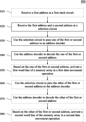
a selection circuit, a latch circuit, and a decoder coupled in series between the read and write ports and the plurality of registers; and
a control circuit configured to, responsive to a clock signal and read and write enable signals, cause the selection circuit, the latch circuit, and the decoder to:
select a first register of the plurality of registers in a read operation based on the read address, and
select a second register of the plurality of registers in a write operation based on the write address.