| CPC G11C 7/1084 (2013.01) [H03K 19/007 (2013.01)] | 20 Claims |
|
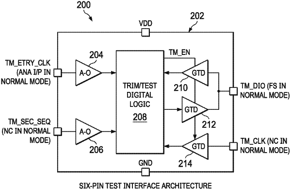
1. A packaged integrated circuit (IC) device comprising:
packaging enclosing an IC die, the packaging comprising conductive pins including a first pin configured to receive analog input signals in a normal mode of the IC device and to receive a digital test mode entry clock signal as a key to entry of the IC device into a test mode in which the IC device is configured to receive test or trim inputs on one or more of the pins and to provide test outputs on the one or more of the pins or to calibrate the IC device by programming trim bit registers in a nonvolatile memory in the IC device, the IC die comprising a power-on reset (POR) generator and a test interface architecture, the test interface architecture comprising:
digital logic configured to transition the IC device from the normal mode to the test mode; and
a floating-pin-tolerant always-on complementary metal-oxide-semiconductor (CMOS) input buffer coupled at a first end to the first pin and at a second end to an input of the digital logic.
|