| CPC G11C 7/1048 (2013.01) [G11C 7/1057 (2013.01); G11C 7/1084 (2013.01); G11C 2207/105 (2013.01)] | 13 Claims |
|
1. An operating method of a storage device including a NAND flash memory device and a controller configured to control the NAND flash memory device, the method comprising:
transmitting a command and an address, via an input/output line, from the controller to the NAND flash memory device;
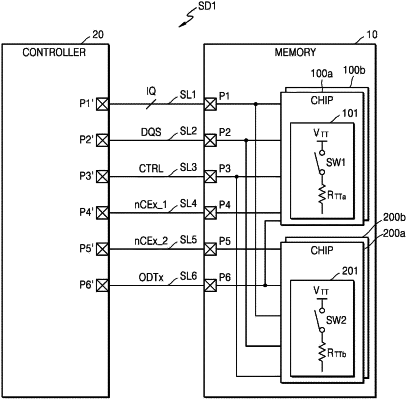
transmitting an on-die Termination (ODT) signal, via a single ODT signal line, from the controller to the NAND flash memory device including a first memory chip including a first ODT circuit, a second memory chip including a second ODT circuit, a third memory chip including a third ODT circuit, and a fourth memory chip including a fourth ODT circuit, the ODT signal defining an enable period for at least one of the first to fourth ODT circuits;
transmitting a first chip enable signal, via a first chip enable signal line, from the controller to the first and second memory chips;
transmitting a second chip enable signal, via a second chip enable signal line, from the controller to the third and fourth memory chips; and
providing a first ODT resistor or a second ODT resistor by the at least one of the first to fourth ODT circuits, in response to the ODT signal, at least one of the first and second chip enable signals, and the address.
|