| CPC G09G 3/32 (2013.01) [H10K 59/1213 (2023.02); H10K 59/1216 (2023.02); G09G 2300/0426 (2013.01); G09G 2300/0819 (2013.01); G09G 2300/0842 (2013.01); G09G 2300/0861 (2013.01); G09G 2310/0267 (2013.01); G09G 2310/0275 (2013.01); G09G 2320/0257 (2013.01); G09G 2330/021 (2013.01); H01L 27/1225 (2013.01); H01L 27/1251 (2013.01); H01L 27/1255 (2013.01); H01L 29/7869 (2013.01); H01L 29/78648 (2013.01); H01L 29/78675 (2013.01)] | 18 Claims |
|
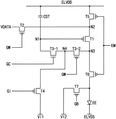
1. A pixel comprising:
a light emitting element;
a driving switching element which applies a driving current to the light emitting element;
a first compensation switching element and a second compensation switching element which are connected between a control electrode of the driving switching element and an output electrode of the driving switching element; and
an initialization switching element which applies an initialization voltage to a node connected between the first compensation switching element and the second compensation switching element,
wherein the first compensation switching element and the second compensation switching element are connected to each other in series,
wherein the driving switching element is a P-type transistor,
wherein the first compensation switching element is an N-type transistor, and
wherein the second compensation switching element is a P-type transistor.
|