| CPC G09G 3/20 (2013.01) [G09G 2310/0267 (2013.01); G09G 2320/0219 (2013.01); G09G 2320/0223 (2013.01); G09G 2330/021 (2013.01)] | 11 Claims |
|
1. A display driving module, comprising a clock signal line, a clock signal generating circuit and a gate driving circuit, wherein the gate driving circuit comprises multiple stages of gate driving units;
the clock signal generating circuit is electrically connected to the clock signal line and is configured to generate at least two clock signals and provide different clock signals to the clock signal line in a time-sharing manner;
the gate driving unit is electrically connected to the clock signal line and configured to generate a gate driving signal according to the clock signals on the clock signal line;
wherein potentials of the clock signals during clock signal intervals corresponding to valid voltages, the potentials of different clock signals are different;
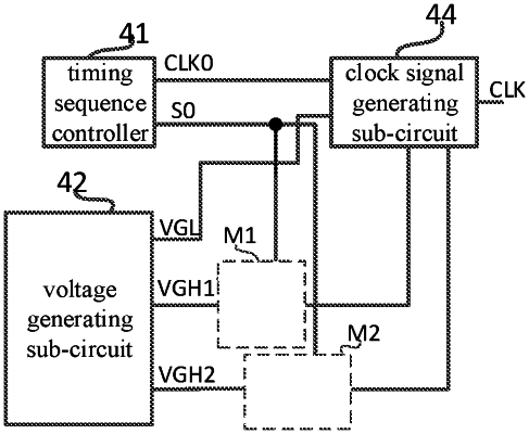
wherein the clock signal generating circuit comprises a timing sequence controller, a voltage generating sub-circuit, a control sub-circuit, and a clock signal generating sub-circuit, wherein
the voltage generating sub-circuit is configured to generate an invalid voltage signal and at least two valid voltage signals and provide the invalid voltage signal to the clock signal generating sub-circuit;
the timing sequence controller is configured to provide a control signal to the control sub-circuit through a control signal end and provide an input clock signal to the clock signal generating sub-circuit through an input clock signal end;
the control sub-circuit is electrically connected to the control signal end and the voltage generating sub-circuit and is configured to provide a corresponding valid voltage signal in the at least two valid voltage signals to the clock signal generating sub-circuit under a control of the control signal;
the clock signal generating sub-circuit is electrically connected to the timing sequence controller, the control sub-circuit, and the clock signal line, and is configured to generate a corresponding clock signal according to the input clock signal, the invalid voltage signal, and the corresponding valid voltage signal, and to provide the clock signal to the clock signal line;
wherein the voltage generating sub-circuit is configured to generate a first valid voltage signal and a second valid voltage signal, and output the first valid voltage signal through a first output end and output the second valid voltage signal through a second output end;
the control sub-circuit comprises a first control transistor and a second control transistor;
a control electrode of the first control transistor is electrically connected to the control signal end, a first electrode of the first control transistor is electrically connected to the first output end, and a second electrode of the first control transistor is electrically connected to the clock signal generating circuit; and
a control electrode of the second control transistor is electrically connected to the control signal end, the first electrode of the second control transistor is electrically connected to the second output end, and the second electrode of the second control transistor is electrically connected to the clock signal generating circuit.
|