| CPC G09G 3/20 (2013.01) [G02F 1/136286 (2013.01); G09G 3/3266 (2013.01); G09G 3/3648 (2013.01); G09G 3/3674 (2013.01); G09G 3/3677 (2013.01); G09G 2230/00 (2013.01); G09G 2300/0408 (2013.01); G09G 2310/0267 (2013.01); G09G 2310/0283 (2013.01); G09G 2310/0286 (2013.01); G09G 2310/0291 (2013.01); G09G 2330/06 (2013.01); G09G 2380/10 (2013.01); G11C 19/28 (2013.01); H10K 59/131 (2023.02)] | 14 Claims |
|
1. A display panel, comprising: a gate drive circuit, a plurality of scan lines and a plurality of inverted scan lines;
wherein the plurality of inverted scan lines is disposed in parallel with the plurality of scan lines;
wherein the gate drive circuit comprises a plurality of cascaded gate drive units, and each of the plurality of gate drive units comprises a shift register unit and an inverted unit;
wherein in a same one of the plurality of gate drive units, the inverted unit is electrically connected to the shift register unit, a scan output terminal of the shift register unit is electrically connected to one of the pluralities of scan lines, and an inverted scan output terminal of the inverted unit is electrically connected to one of the plurality of inverted scan lines;
wherein the scan output terminal of the shift register unit outputs a first effective pulse signal, and the inverted scan output terminal of the inverted unit outputs a second effective pulse signal;
wherein a time period corresponding to the first effective pulse signal completely overlaps a time period corresponding to the second effective pulse signal, and a level state of the first effective pulse signal is opposite to a level state of the second effective pulse signal;
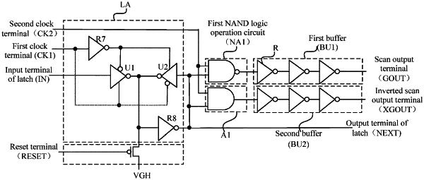
wherein the shift register unit comprises: a latch, a first NAND logic operation circuit and a first buffer; wherein a clock input terminal of the latch is electrically connected to a first clock terminal of the display panel, and an input terminal of the latch is electrically connected to an output terminal of a latch in an upper-stage shift register unit of the shift register unit;
wherein a first input terminal of the first NAND logic operation circuit is electrically connected to an output terminal of the latch, a second input terminal of the first NAND logic operation circuit is electrically connected to a second clock terminal of the display panel, an output terminal of the first NAND logic operation circuit is electrically connected to an input terminal of the first buffer, and an output terminal of the first buffer is connected to the one of the plurality of scan lines;
wherein the inverted unit comprises a first AND logic operation circuit and a second buffer, wherein a first input terminal of the first AND logic operation circuit is electrically connected to the output terminal of the latch, a second input terminal of the first AND logic operation circuit is electrically connected to the second clock terminal of the display panel, an output terminal of the first AND logic operation circuit is electrically connected to an input terminal of the second buffer, and an output terminal of the second buffer is connected to the one of the plurality of inverted scan lines; and
wherein the first buffer and the second buffer each comprises m inverters connected in series, wherein m is a positive integer.
|