| CPC G06K 19/07722 (2013.01) [B23C 3/13 (2013.01); B32B 38/10 (2013.01); G06K 19/07775 (2013.01); B32B 2425/00 (2013.01)] | 11 Claims |
|
1. A metal card manufacturing method comprising:
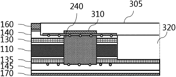
forming a metal card by laminating stacked sheets comprising a plurality of sheets having a metal sheet at a center thereof, wherein the stacked sheets include one or more adhesive sheets having a same size as that of the metal sheet, an upper inlay sheet having a first antenna formed thereon, and a lower inlay sheet having a second antenna formed thereon;
forming a COB (Chip On Board) accommodation space capable of accommodating a COB by milling a predetermined area of the metal card through a computerized numerical control (CNC) machining process;
forming a through-hole exposing the first antenna and the second antenna by milling a COB contact point area of the COB accommodation space as deep as the lower inlay sheet;
electrically connecting the first antenna and the second antenna by dispensing a conductive elastic liquid inside the through-hole; and
bidirectionally connecting the first antenna and the second antenna to the COB by attaching the COB in the COB accommodation space so that contact points of the COB are connected by the conductive elastic liquid,
wherein the forming the COB accommodation space comprises:
performing a primary milling to a first depth to expose an upper inlay sheet area corresponding to a COB pad area for inserting the COB; and
performing secondary milling on an area corresponding to a COB chip area to a second depth to form a COB chip accommodation unit in the COB pad area,
wherein the forming a through-hole comprises:
cutting to a third depth by performing an adjusted tertiary milling of the COB accommodation space until at least a part of the first antenna corresponding to the COB contact point area is exposed for connection of the contact points of the COB; and
processing to form the through-hole by performing a quaternary milling on a tertiary-milled area until at least a part of the second antenna of the lower inlay sheet is exposed, and
wherein the at least a part of the first antenna of the upper inlay layer and the at least a part of the second antenna of the lower inlay layer are both exposed through the formed through-hole.
|