| CPC G06F 1/06 (2013.01) [H03K 3/86 (2013.01); H03K 5/05 (2013.01); H03K 5/06 (2013.01); H03K 19/1776 (2013.01)] | 15 Claims |
|
1. A clock generation circuit, comprising:
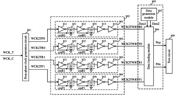
a four-phase clock generation circuit for receiving an internal clock signal and a complementary clock signal of a memory to which the clock generation circuit belongs, configured to generate a first clock signal, a second clock signal, a third clock signal, and a fourth clock signal with a same cycle based on the internal clock signal and the complementary clock signal, wherein
the internal clock signal and the complementary clock signal are reverse signals, a cycle of the first clock signal is K times a cycle of the internal clock signal, K is a positive integer, and a value of K depends on a signal delay inside the four-phase clock generation circuit;
a signal delay circuit for receiving the first clock signal, the second clock signal, the third clock signal, the fourth clock signal, and a delay command, configured to perform signal delay on the first clock signal, the second clock signal, the third clock signal, and the fourth clock signal respectively based on the delay command, wherein delays of the first clock signal, the second clock signal, the third clock signal, and the fourth clock signal are different;
a signal loading circuit, connected to the signal delay circuit, and configured to generate a first indication signal and a second indication signal based on the delayed first clock signal, the delayed second clock signal, the delayed third clock signal, and the delayed fourth clock signal; and
a test circuit, connected to the signal loading circuit, and configured to perform a duty cycle test based on the first indication signal and the second indication signal.
|