| CPC G05F 1/56 (2013.01) | 20 Claims |
|
1. A method comprising:
receiving a main supply voltage;
generating a first regulated output voltage with a DC-DC converter;
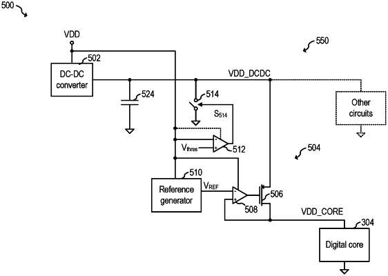
providing the main supply voltage to a supply terminal of a driver, the driver having an output coupled to a control terminal of an output transistor of an LDO, the main supply voltage used to power the driver, the LDO having an input terminal coupled to a first current path terminal of the output transistor, and an output terminal coupled to second current path terminal of the output transistor;
receiving, at the input terminal of the LDO, the first regulated output voltage;
generating, at the output terminal of the LDO, a second regulated output voltage from the first regulated output voltage; and
in response to the main supply voltage falling below a predetermined threshold, discharging a capacitor coupled to the input terminal of the LDO by activating a switch coupled to the input terminal of the LDO.
|