| CPC G03F 7/30 (2013.01) [G03F 7/0045 (2013.01); G03F 7/0382 (2013.01); G03F 7/0392 (2013.01); G03F 7/0397 (2013.01); G03F 7/2004 (2013.01); G03F 7/32 (2013.01); G03F 7/36 (2013.01); G03F 7/38 (2013.01); G03F 7/40 (2013.01); B82Y 30/00 (2013.01); B82Y 40/00 (2013.01)] | 20 Claims |
|
1. A method of manufacturing a semiconductor device, comprising:
forming a photoresist layer comprising a photoresist composition over a substrate;
selectively exposing the photoresist layer to actinic radiation to form a latent pattern; and
developing the latent pattern by applying a developer to the selectively exposed photoresist layer to form a pattern,
wherein the photoresist composition comprises:
a photoactive compound; and
a polymer,
wherein the polymer has a polymer backbone comprising one or more groups selected from:
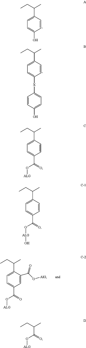 and wherein the polymer backbone includes at least one group selected from B, C-1, or C-2,
ALG is an acid labile group, and
X is a linking group.
|