| CPC G02B 26/0833 (2013.01) [B82Y 20/00 (2013.01); G02B 5/003 (2013.01); G02B 26/001 (2013.01); G02F 1/133502 (2013.01); B60J 3/06 (2013.01); G02F 1/0063 (2013.01); G02F 2201/38 (2013.01); G02F 2201/40 (2013.01)] | 20 Claims |
|
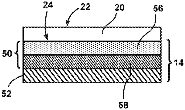
1. An aperture structure for a substrate of an optical device, comprising:
an optical cavity layer that comprises a dielectric material comprising at least one of a metal oxide, a metal nitride, and a metal oxynitride, the optical cavity layer further comprising a refractive index of about 1.4 or greater, as measured at a wavelength of 550 nm; a transmittance of at least about 50% for each wavelength of light in the range from 400 nm to 700 nm at each angle of incidence from 0 degrees to 30 degrees; and a thickness of about 10 nm to about 200 nm;
a light absorbing layer disposed over the optical cavity layer, the light absorbing layer comprising a metal or a metal alloy; an extinction coefficient k of at least 1, as measured at a wavelength of 550 nm; and a thickness of about 3 nm to about 60 nm; and
a blocking layer disposed over the light absorbing layer, the blocking layer comprising a metal or a metal alloy; an optical density of at least 3 at each wavelength of light in the range from 400 nm to 700 nm; and a thickness of about 30 nm to about 300 nm;
wherein the aperture structure comprises a reflectance of less than 5% for each wavelength of light in the range from 400 nm to 700 nm at each angle of incidence from 0 degrees to 30 degrees, as measured through the substrate.
|