| CPC G02B 6/13 (2013.01) [G02B 6/12002 (2013.01); H01L 21/0245 (2013.01); H01L 21/0262 (2013.01); H01L 21/02381 (2013.01); H01L 21/02505 (2013.01); H01L 21/02532 (2013.01); H01L 21/02573 (2013.01); H01L 21/02639 (2013.01); H01L 21/2033 (2013.01); H01L 21/2053 (2013.01); H01L 27/14625 (2013.01); H01L 31/028 (2013.01); H01L 31/0232 (2013.01); H01L 31/02327 (2013.01); H01L 31/022408 (2013.01); H01L 31/105 (2013.01); H01L 31/1808 (2013.01); G02B 6/132 (2013.01); G02B 6/136 (2013.01); G02B 6/1347 (2013.01); G02B 6/43 (2013.01); G02B 2006/121 (2013.01); G02B 2006/12061 (2013.01); G02B 2006/12104 (2013.01); G02B 2006/12123 (2013.01); G02B 2006/12169 (2013.01); H01L 27/14629 (2013.01); Y02E 10/52 (2013.01); Y02E 10/547 (2013.01)] | 21 Claims |
|
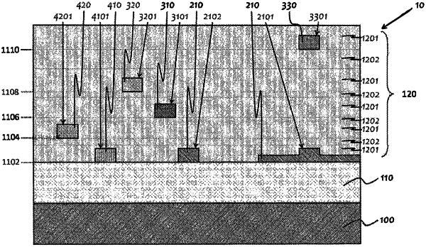
1. A photonic structure, comprising:
a plurality of photonic layers formed on a substrate, wherein the plurality of photonic layers includes a first photonic layer and a second photonic layer;
wherein the first photonic layer and the second photonic layer are each patterned such that each of the first photonic layer and the second photonic layer defines one or more sets of photonic features; and
wherein the first photonic layer and the second photonic layer are each formed of a distinct waveguiding material and wherein the first photonic layer and the second photonic layer are at a common elevation on the substrate.
|