| CPC G02B 6/124 (2013.01) [G02B 6/136 (2013.01); H01L 23/48 (2013.01); G02B 6/12002 (2013.01); G02B 6/12004 (2013.01); G02B 6/12019 (2013.01)] | 20 Claims |
|
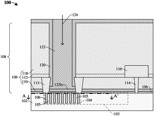
1. A method for forming an integrated chip, the method comprising:
forming a waveguide on a first surface of a substrate;
forming a conductive structure at least partially overlying the waveguide; and
forming a light pipe structure over the waveguide, wherein a lower surface of the light pipe structure is disposed between a top surface and a bottom surface of the conductive structure, and wherein a lower portion of the light pipe structure contacts the conductive structure.
|