| CPC G01R 31/2891 (2013.01) [G01R 31/2887 (2013.01); H01L 22/12 (2013.01)] | 7 Claims |
|
1. A semiconductor inspecting method for ensuring scrubbing length on pad, comprising multiple steps of:
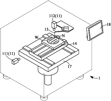
(a) getting an image from above a probe needle by adopting a vision system of a semiconductor inspecting system, the image at least comprising the probe needle, and defining a first position of the probe needle in the image wherein a wafer comprising at least a pad is placed on a wafer chuck of a semiconductor inspecting system;
(b) making a relative vertical movement between the probe needle and the pad by adopting a driving system of the semiconductor inspecting system to generate a second position of the probe needle in the image, and to make the probe needle scrub a scrubbing length on the pad, wherein the second position is defined as a changed position in the image corresponding to the first position of the probe needle in the image after the relative vertical movement, the changed position caused by the probe needle being contacted with the pad to generate the scrubbing length on the pad;
(c) calculating the scrubbing length depending on recognizing a difference in the image between the second position and the first position by adopting the vision system; and
(d) continuing making the relative vertical movement between the probe needle and the pad until the scrubbing length is equal to or larger than a preset value, and then stopping the relative vertical movement by adopting the driving system.
|