| CPC G01R 31/2841 (2013.01) [G01R 31/2843 (2013.01); H04B 3/46 (2013.01)] | 20 Claims |
|
1. A manufacturing method of an electronic device, comprising:
providing a substrate;
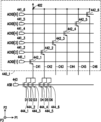
forming a plurality of signal lines and a testing circuit on the substrate, wherein the testing circuit comprises a plurality of output channels electrically connected to some of the plurality of signal lines, and the testing circuit comprises a plurality of switches and a plurality of sub-testing circuits, wherein the plurality of switches are connected to the plurality of signal lines via the plurality of sub-testing circuits;
performing a testing process, comprising:
providing a signal;
processing the signal to form a plurality of testing signals by the testing circuit, comprising:
turning on a first switch of the plurality of switches and turning off the other switches of the plurality of switches according to a plurality of control signals, wherein the first switch is electrically connected to the some of plurality of signal lines; and
transmitting the plurality of testing signals to the some of the plurality of signal lines via the plurality of output channels; and
optionally isolating the testing circuit from the some of the plurality of signal lines,
wherein the overall plurality of output channels of the testing circuit are less than the overall plurality of signal lines in quantity.
|