| CPC G01R 19/32 (2013.01) [H02M 3/07 (2013.01); G11C 11/4074 (2013.01)] | 18 Claims |
|
1. A voltage detection circuit, comprising:
a voltage raising circuit configured to adjust a voltage to be measured and output an adjusted voltage, wherein the adjusted voltage is equal to a sum of the voltage to be measured and a reference voltage; and
a current generation circuit connected to the voltage raising circuit and configured to provide a constant current to the voltage raising circuit,
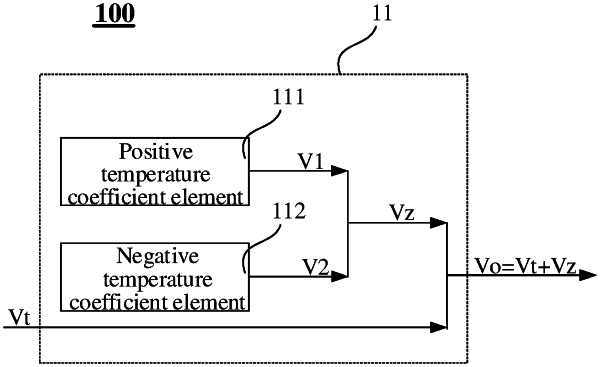
wherein the reference voltage is generated by a combination of a first voltage with a positive temperature coefficient and a second voltage with a negative temperature coefficient, and
wherein the current generation circuit comprises:
a first switch transistor having a first terminal connected to a power supply voltage, a second terminal connected with a first node, and a control terminal connected with a second node;
a second switch transistor having a first terminal connected to the power supply voltage, a second terminal connected with a third node, and a control terminal connected with the second node;
a third switch transistor having a first terminal connected to the power supply voltage, a control terminal connected with the second node, and a second terminal configured to output the constant current;
a first bipolar transistor having an emitter connected with the first node through a first resistor, and a collector and a base that are grounded;
a second bipolar transistor having an emitter connected with the third node, and a collector and a base that are grounded; and
an amplifier having a non-inverting input terminal connected with the first node, an inverting input terminal connected with the third node, and an output terminal connected with the second node.
|