| CPC G01N 21/9501 (2013.01) [H01L 22/12 (2013.01); H01L 22/24 (2013.01); G01N 21/3563 (2013.01); G01N 2021/1776 (2013.01); G01N 2021/3568 (2013.01)] | 23 Claims |
|
1. A system, comprising:
a plurality of wafer inspection system (WIS) modules for monitoring one or more characteristics of a substrate, wherein each WIS module comprises:
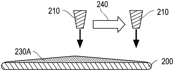
a camera system configured to obtain multiple spectral band values from the substrate when the substrate is disposed within each of the WIS modules; and
a controller coupled to receive the multiple spectral band values from the camera system, each of the multiple spectral band values being associated with a calculated light intensity across a band of wavelength, wherein the controller is configured to apply multiple spectral band offset values to the multiple spectral band values received from the camera system to generate calibrated multiple spectral band values, which compensate for spectral responsivity differences between the camera systems included within the plurality of WIS modules, wherein different ones of the multiple spectral band offset values are applied to different bands of wavelengths.
|