| CPC C23C 16/4404 (2013.01) [C23C 16/401 (2013.01); C23C 16/4405 (2013.01); C23C 16/45557 (2013.01); H01J 37/32477 (2013.01); H01J 37/32853 (2013.01); H01J 37/32862 (2013.01)] | 20 Claims |
|
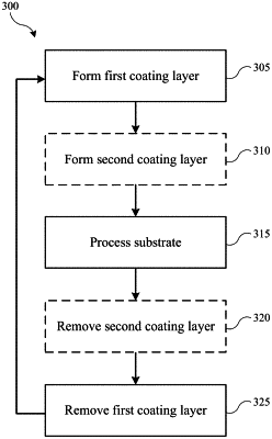
1. A method of semiconductor processing, the method comprising:
performing a first plasma treatment within a processing chamber to remove a first carbon-containing material;
performing a second plasma treatment within the processing chamber to remove a first silicon-containing material;
increasing a processing pressure between performing the first plasma treatment and performing the second plasma treatment;
depositing a second silicon-containing material on surfaces of the processing chamber, wherein the second silicon-containing material is characterized by a water contact angle of greater than or about 90°; and
depositing a second carbon-containing material overlying the second silicon-containing material.
|