| CPC B41J 2/14024 (2013.01) [B41J 2/14072 (2013.01); B41J 2/14129 (2013.01); B41J 2/14088 (2013.01); B41J 2/155 (2013.01); B41J 2/1635 (2013.01); B41J 2/21 (2013.01); B41J 2202/11 (2013.01); B41J 2202/13 (2013.01)] | 20 Claims |
|
1. A wafer structure, comprising:
a chip substrate being a silicon substrate and fabricated by a semiconductor process on a wafer of at least 12 inches; and
a plurality of inkjet chips comprising at least one first inkjet chip and at least one second inkjet chip directly formed on the chip substrate by the semiconductor process, respectively, whereby the plurality of inkjet chips are diced into the at least one first inkjet chip and the at least one second inkjet chip, to be implemented for inkjet printing, wherein a size of a printing swath of the at least one first inkjet chip is different from a size of a printing swath of the at least one second inkjet chip,
wherein each of the at least one first inkjet chip and the at least one second inkjet chip further comprises:
at least one ink-supply channel configured to provide ink; and
a plurality of ink-drop generators respectively connected to the at least one ink-supply channel,
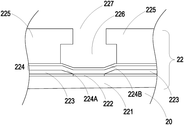
wherein each of the ink-drop generators comprises a thermal-barrier layer, a resistance heating layer, only one conductive layer, a protective layer, a barrier layer, an ink-supply chamber and a nozzle, wherein the conductive layer and a part of the protective layer are formed on the resistance heating layer, a rest part of the protective layer is formed on the conductive layer, the barrier layer is directly formed on the protective layer, the ink-supply chamber and the nozzle are integrally formed in the barrier layer, the ink-supply chamber has a bottom in communication with the protective layer, and a top in communication with the nozzle,
wherein the barrier layer includes two opposite inner sidewalls defining two opposite sides of the ink-supply chamber, each of the two opposite inner sidewalls of the barrier layer continuously extends from a respective one of two opposite sides of a top surface of a continuous portion of the protective layer toward the nozzle, the two opposite inner sidewalls of the barrier layer entirely and directly overlap with the conductive layer in a direction normal to the bottom of the ink-supply chamber, and the top surface of the continuous portion of the protective layer is the bottom of the ink-supply chamber, and
wherein an ink supply path is formed between the at least one ink-supply channel and the ink-supply chamber of each of the plurality of ink-drop generators, and the ink supply path is configured to supply the ink from the at least one ink-supply channel to the ink-supply chamber in a plane parallel with the bottom of the ink supply chamber.
|