| CPC B41J 2/04551 (2013.01) [B41J 2/0458 (2013.01); B41J 2/04541 (2013.01); B41J 2/04543 (2013.01); B41J 2/04581 (2013.01); B41J 2/1433 (2013.01); B41J 2/14072 (2013.01); B41J 2/14201 (2013.01); G11C 7/1072 (2013.01); B41J 2002/14491 (2013.01)] | 9 Claims |
|
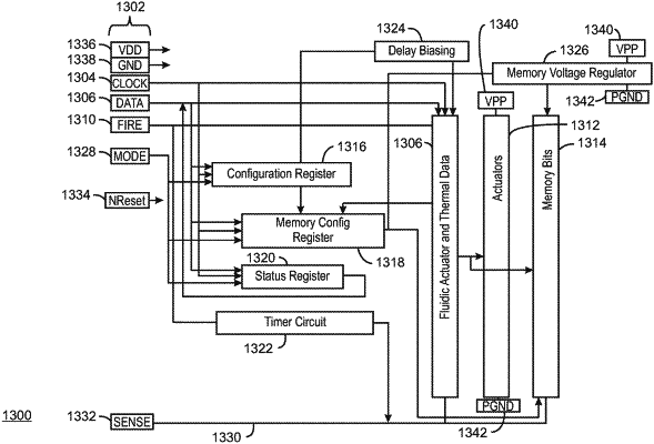
1. A die for a printhead, comprising:
a configuration register;
a memory configuration register to operate parallel to the configuration register;
a plurality of fluidic actuator arrays;
a power line and a separate activation signal line routed across a feed zone of the die;
data blocks in a data store coupled to the memory configuration register, the data blocks comprising a data block associated with each of the plurality of fluidic actuator arrays; and
an interface comprising a data pad and a clock pad, wherein the data blocks are configured so that a data bit value present at the data pad is loaded into a first data block corresponding to a first fluidic actuator array on a rising clock edge and loaded into a second data block corresponding to a second fluidic actuator array on a falling clock edge.
|