| CPC B23K 26/36 (2013.01) [H01L 21/302 (2013.01); H01L 21/82 (2013.01); B23K 2103/56 (2018.08); H01L 23/544 (2013.01)] | 11 Claims |
|
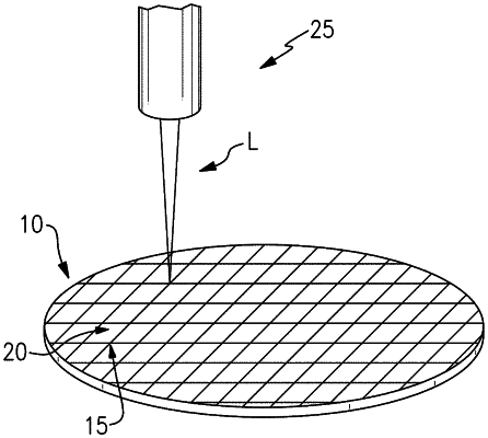
1. A method of separating plurality of integrated circuit dies from a wafer, comprising:
making a first plurality of cutting passes consisting of only three cutting passes in a same first direction with a laser along a first die street of an integrated circuit die of the plurality of integrated circuit dies, the first die street extending along a first axis on the wafer; and
making a second plurality of cutting passes consisting of only three cutting passes in a same second direction with the laser along a second die street of the integrated circuit die, the second die street extending along a second axis on the wafer being generally perpendicular to the first axis, and
the first plurality of cutting passes along the first die street being altematingly and consecutively made with the second plurality of cutting passes along the second die street to thereby fully separate the integrated circuit die from the wafer along the first and second axes, the making of the first plurality and the second plurality of cutting passes with the laser along the first and second die streets on the wafer including cutting with the laser at a same power level along the first and second die streets.
|