US 11,683,991 B2
Semiconductor structure and manufacturing method of the same
Tai-Yen Peng, Hsinchu (TW); Yu-Shu Chen, Hsinchu (TW); Chien Chung Huang, Taichung (TW); Sin-Yi Yang, Taichung (TW); Chen-Jung Wang, Hsinchu (TW); Han-Ting Lin, Hsinchu (TW); Jyu-Horng Shieh, Hsin-Chu (TW); and Qiang Fu, Hsinchu (TW)
Assigned to TAIWAN SEMICONDUCTOR MANUFACTURING COMPANY LTD., Hsinchu (TW)
Filed by TAIWAN SEMICONDUCTOR MANUFACTURING COMPANY LTD., Hsinchu (TW)
Filed on Nov. 24, 2020, as Appl. No. 17/103,577.
Application 17/103,577 is a division of application No. 16/242,689, filed on Jan. 8, 2019, granted, now 10,862,023.
Claims priority of provisional application 62/711,803, filed on Jul. 30, 2018.
Prior Publication US 2021/0074909 A1, Mar. 11, 2021
Int. Cl. H10N 50/80 (2023.01); H10N 50/01 (2023.01); H10N 50/85 (2023.01); H01L 43/02 (2006.01); H01L 43/12 (2006.01); H01L 43/10 (2006.01)
CPC H01L 43/02 (2013.01) [H01L 43/10 (2013.01); H01L 43/12 (2013.01)] 20 Claims
OG exemplary drawing
 
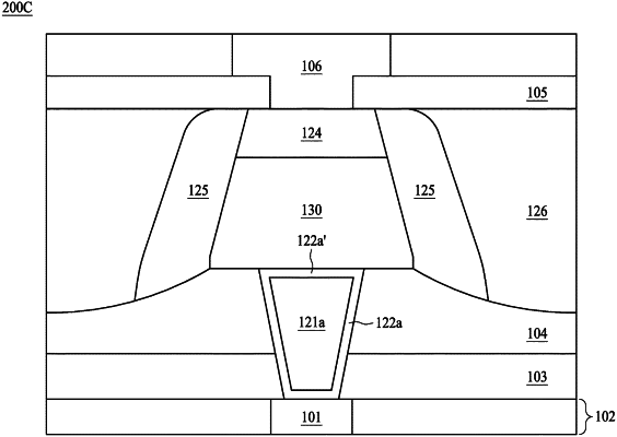
1. A method for manufacturing semiconductor structure, the method comprising:
forming an insulation layer;
forming a first via trench in the insulation layer;
forming a barrier layer in the first via trench;
forming a bottom electrode via in the first via trench;
forming a magnetic tunneling junction (MTJ) layer above the bottom electrode via; and
performing an ion beam etching operation, comprising
patterning the MTJ layer to form an MTJ; and
removing a portion of the insulation layer from a top surface.