| CPC H10B 63/80 (2023.02) [G11C 13/0004 (2013.01); G11C 13/0007 (2013.01); H10N 70/231 (2023.02); H10N 70/8822 (2023.02); H10N 70/8825 (2023.02); H10N 70/8828 (2023.02); G11C 2213/76 (2013.01)] | 15 Claims |
|
1. A memory device comprising:
a first conductive layer;
a second conductive layer;
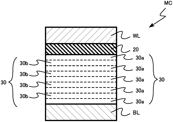
a resistance change region provided between the first conductive layer and the second conductive layer;
a first region provided between the resistance change region and the first conductive layer, the first region including a first element selected from the group consisting of niobium (Nb), vanadium (V), tantalum (Ta), and titanium (Ti), and a second element selected from the group consisting of oxygen (O), sulfur (S), selenium (Se), and tellurium (Te), the first region having a first atomic ratio of the first element to the second element; and
a second region provided between the first region and the resistance change region, the second region including the first element and the second element, the second region having a second atomic ratio of the first element to the second element, the second atomic ratio being smaller than the first atomic ratio.
|