| CPC H10B 10/125 (2023.02) [H01L 23/528 (2013.01)] | 20 Claims |
|
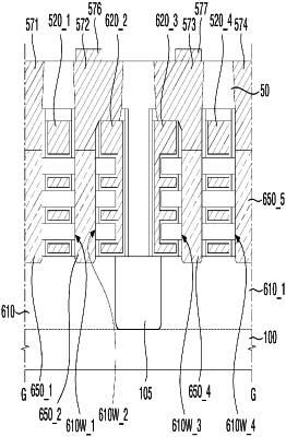
1. A semiconductor device comprising:
a first fin type pattern extending lengthwise in a first direction;
a second fin type pattern extending lengthwise in the first direction and spaced apart from the first fin type pattern in a second direction from the first direction;
a first gate pattern and a second gate pattern intersecting the first fin type pattern and the second fin type pattern;
a third gate pattern and a fourth gate pattern intersecting the first fin type pattern between the first gate pattern and the second gate pattern;
a fifth gate pattern and a sixth gate pattern intersecting the second fin type pattern between the first gate pattern and the second gate pattern;
a first semiconductor pattern between the fifth gate pattern and the sixth gate pattern, on the second fin type pattern; and
a gate cut structure separating the third and fourth gate patterns and the fifth and sixth gate patterns,
wherein the first semiconductor pattern is electrically floating.
|