| CPC H04N 25/75 (2023.01) [H04N 25/709 (2023.01); H04N 25/772 (2023.01)] | 18 Claims |
|
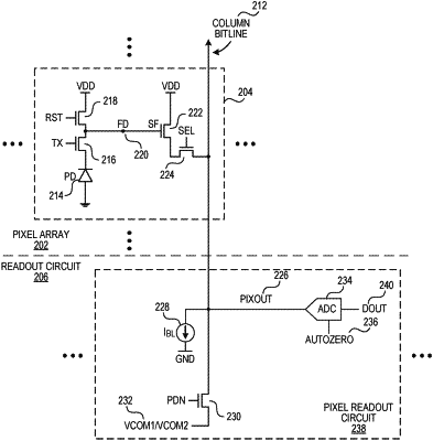
1. A pixel readout circuit, comprising:
an analog to digital converter coupled to the bitline output of the pixel circuit; and
a switch coupled between the bitline output of the pixel circuit and a reference voltage,
wherein the switch is configured to be pulsed on and off a first time to settle the bitline to the reference voltage prior to an autozero operation of the analog to digital converter for each readout of the pixel circuit,
wherein the switch is configured to be pulsed on and off a second time to settle the bitline to the reference voltage after the autozero operation and prior to a first analog to digital conversion operation of the analog to digital converter for each readout of the pixel circuit,
wherein the switch is configured to be pulsed on and off a third time to settle the bitline to the reference voltage after the first analog to digital conversion operation and prior to a second analog to digital conversion operation of the analog to digital converter for each readout of the pixel circuit.
|