| CPC H04N 25/75 (2023.01) [H01L 27/14612 (2013.01); H01L 27/14643 (2013.01); H01L 27/14831 (2013.01); H04N 25/704 (2023.01); H04N 25/772 (2023.01)] | 13 Claims |
|
1. An imaging device, comprising:
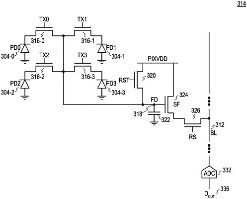
a plurality of photodiodes arranged in a photodiode array to generate charge in response to incident light, wherein the plurality of photodiodes includes a first photodiode, a second photodiode, a third photodiode, and a fourth photodiode;
a shared floating diffusion configured to receive charge transferred from the first, second, third, and fourth photodiodes;
a plurality of transfer transistors, wherein each one of the plurality of transfer transistors is coupled to a corresponding one of the plurality photodiodes, wherein the plurality of transfer transistors includes a first transfer transistor coupled between the first photodiode and the shared floating diffusion, a second transfer transistor coupled between the second photodiode and the shared floating diffusion, a third transfer transistor coupled between the third photodiode and the shared floating diffusion, and a fourth transfer transistor coupled between the fourth photodiode and the shared floating diffusion;
a reset transistor coupled between the shared floating diffusion and a voltage supply;
a source follower transistor having a gate coupled to the shared floating diffusion and a source coupled to a column bitline;
a row select transistor coupled to the source follower transistor, wherein the source follower transistor and the row select transistor are coupled between the voltage supply and the column bitline; and
an analog to digital converter (ADC) coupled to the column bitline, wherein the ADC is configured to perform a first ADC conversion to generate a reference readout in response to charge in the shared floating diffusion after a reset operation, wherein the reset operation is configured to be performed in response to the reset transistor being pulsed while simultaneously the first, second, third, and fourth transfer transistors are turned off to reset the shared floating diffusion, wherein the ADC is next configured to perform a second ADC conversion to generate a first half of a phase detection autofocus (PDAF) readout in response to the first and third transfer transistors being pulsed simultaneously while simultaneously the reset transistor and the second and fourth transfer transistors are turned off to transfer charge from the first and third photodiodes to the shared floating diffusion, wherein the ADC is then configured to perform a third ADC conversion to generate a full image readout in response to the second and fourth transfer transistors being pulsed simultaneously while simultaneously the reset transistor and the first and third transfer transistors are turned off to combine the charge transferred previously from the first and third photodiodes in the shared floating diffusion with charge transferred from the second and fourth photodiodes.
|