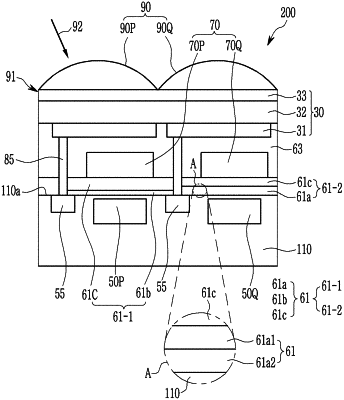
| CPC H04N 25/17 (2023.01) [H01L 27/14621 (2013.01); H01L 27/14627 (2013.01); H01L 27/14629 (2013.01); H04N 5/32 (2013.01)] | 20 Claims |

|
1. An image sensor, comprising:
a photoelectric device on a semiconductor substrate, the photoelectric device including
a first electrode and a second electrode facing each other, wherein one of the first electrode or the second electrode is an anode and another one of the first electrode or the second electrode is a cathode, wherein each of the first electrode and the second electrode is a light-transmitting electrode that includes one of
a transparent conductor, or
a metal thin layer, or
a metal thin layer doped with a metal oxide, and
an active layer between the first electrode and the second electrode, the active layer configured to selectively absorb light associated with a first wavelength spectrum to generate excitons that are separated into holes and electrons and to cause a photoelectric effect to be generated based on the separated holes being transferred to the anode and the separated electrons being transferred to the cathode, the first wavelength spectrum associated with a first color of three primary colors;
a first photo-sensing device stacked with the photoelectric device such that the photoelectric device overlaps the first photo-sensing device in a vertical direction extending orthogonally with an upper surface of the semiconductor substrate, the first photo-sensing device configured to sense light associated with a second wavelength spectrum, the second wavelength spectrum associated with a second color of the three primary colors;
a second photo-sensing device stacked with the photoelectric device such that the photoelectric device overlaps the second photo-sensing device in the vertical direction, the second photo-sensing device configured to sense light associated with a third wavelength spectrum, the third wavelength spectrum associated with a third color of the three primary colors;
a first color filter between the photoelectric device and the first photo-sensing device in the vertical direction and configured to selectively transmit light associated with the second wavelength spectrum;
a second color filter between the photoelectric device and the second photo-sensing device in the vertical direction and configured to selectively transmit light associated with the first wavelength spectrum and the third wavelength spectrum; and
a first insulating layer between the photoelectric device and the second photo-sensing device in the vertical direction and configured to selectively reflect light of wavelength spectra except for light associated with the third wavelength spectrum.
|