| CPC H03F 1/3205 (2013.01) [H03F 3/2173 (2013.01); H03F 2200/03 (2013.01); H03F 2200/165 (2013.01); H03F 2200/351 (2013.01)] | 27 Claims |
|
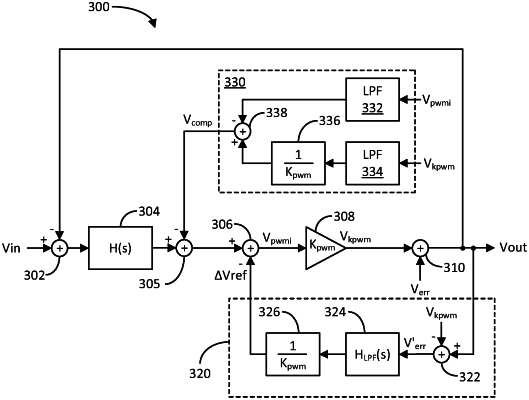
1. An apparatus, comprising:
a pulse width modulator including an input configured to receive a first signal based on an input signal, and an output configured to generate a pulse width modulated (PWM) signal;
an H-bridge including an input coupled to the output of the pulse width modulator and an output coupled to a load, wherein the H-bridge is configured to generate an output signal across the load based on the PWM signal; and
a deadtime compensation circuit coupled to the H-bridge, wherein the deadtime compensation circuit is configured to compensate for deadtime distortion in the output signal, wherein the deadtime compensation circuit is coupled between the output of the H-bridge and the input of the pulse width modulator, and wherein the deadtime compensation circuit comprises:
a first signal subtractor including a first input coupled to the output of the H-bridge, and a second input coupled to the output of the pulse width modulator;
a low pass filter including an input coupled to an output of the first signal subtractor; and
a signal scalar including an input coupled to an output of the low pass filter and an output coupled to the input of the pulse width modulator.
|