| CPC H01L 33/486 (2013.01) [H01L 27/156 (2013.01); H01L 29/7869 (2013.01); H01L 33/12 (2013.01); H01L 33/38 (2013.01); H01L 33/40 (2013.01); H01L 33/62 (2013.01)] | 22 Claims |
|
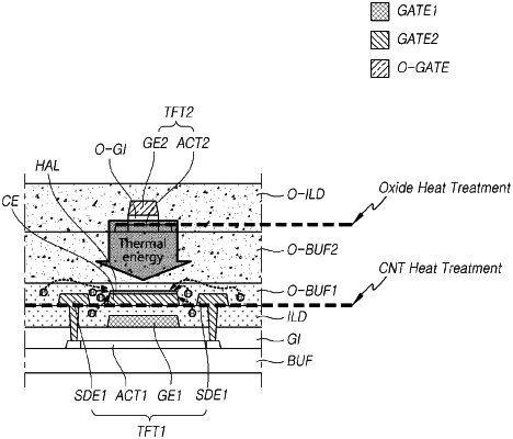
1. A display device comprising:
a plurality of first thin film transistors disposed on a substrate;
at least one insulation layer disposed on at least one of the plurality of first thin film transistors;
a plurality of second thin film transistors disposed on the at least one insulation layer; and
a capacitor electrode including a hydrogen adsorption layer disposed between at least some first thin film transistors among the plurality of first thin film transistors and the at least one insulation layer and disposed on at least one of upper and lower surfaces of the capacitor electrode,
wherein the at least one insulation layer includes:
an interlayer insulation layer disposed on a gate electrode of one of the plurality of first thin film transistors,
a first buffer layer disposed on the interlayer insulation layer, and
a second buffer layer disposed on the first buffer layer and made of a different material from the first buffer layer,
wherein the capacitor electrode is disposed between the interlayer insulation layer and the first buffer layer.
|