| CPC H01L 29/785 (2013.01) [H01L 23/528 (2013.01); H01L 23/5226 (2013.01); H01L 29/41791 (2013.01); H01L 29/42372 (2013.01); H01L 29/4975 (2013.01); H01L 29/66795 (2013.01); H01L 2029/7858 (2013.01)] | 20 Claims |
|
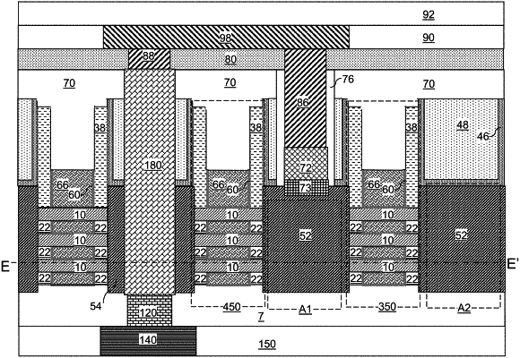
1. A device structure comprising:
a semiconductor nanostructure located on a front surface of an backside insulating matrix layer and comprising:
at least one semiconductor channel plate;
a gate structure; and
a first active region and a second active region located at end portions of the at least one semiconductor channel plate and comprising a source region and a drain region;
an epitaxial semiconductor material portion laterally spaced from the semiconductor nanostructure and overlying the backside insulating matrix layer;
a layer stack including, from bottom to top, a planarization dielectric layer and a via-level dielectric layer and overlying the semiconductor nanostructure and the epitaxial semiconductor material portion;
a backside metal interconnect structure located on a bottom surface of the backside insulating matrix layer; and
an electrically conductive path connecting the first active region and the backside metal interconnect structure and comprising a connector via structure in contact with a sidewall of the epitaxial semiconductor material portion and having a top surface within a horizontal plane including an interface between the planarization dielectric layer and the via-level dielectric layer.
|