| CPC H01L 29/7824 (2013.01) [H01L 29/0649 (2013.01); H01L 29/1079 (2013.01); H01L 29/517 (2013.01); H01L 29/66689 (2013.01)] | 10 Claims |
|
1. A high voltage semiconductor device, comprising:
a semiconductor substrate comprising a channel region;
an isolation structure, wherein at least a part of the isolation structure is disposed in the semiconductor substrate and surrounds the channel region;
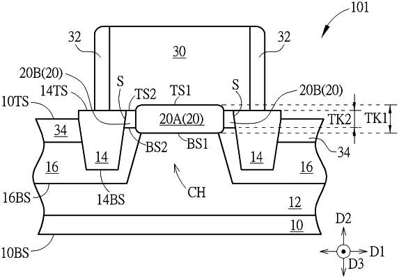
a gate oxide layer disposed on the semiconductor substrate, wherein the gate oxide layer comprises:
a first portion; and
a second portion disposed at two opposite sides of the first portion in a horizontal direction, wherein a thickness of the first portion is greater than a thickness of the second portion;
a gate structure disposed on the gate oxide layer and the isolation structure; and
two drift regions disposed in the semiconductor substrate and located at two opposite sides of the channel region in the horizontal direction respectively, wherein at least a part of the isolation structure is disposed in the two drift regions, and a part of each of the two drift regions is located between the isolation structure and the first portion of the gate oxide layer in the horizontal direction and located beneath the second portion of the gate oxide layer in a vertical direction perpendicular to the horizontal direction.
|