| CPC H01L 29/778 (2013.01) [H01L 21/02573 (2013.01); H01L 21/28 (2013.01); H01L 29/45 (2013.01); H01L 29/49 (2013.01); H01L 29/6653 (2013.01); H01L 29/786 (2013.01)] | 13 Claims |
|
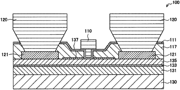
1. A switching transistor, comprising:
a channel layer including a compound semiconductor and having sheet electron density that is equal to or higher than 1.7×1013 cm−2;
a barrier layer on the channel layer, wherein the barrier layer includes a compound semiconductor that is of a different type from the channel layer;
a back-barrier layer inside the channel layer, wherein
the back-barrier layer includes a compound semiconductor similar to the barrier layer;
a gate electrode on the barrier layer;
a source electrode and a drain electrode on the barrier layer, wherein the gate electrode is between the source electrode and the drain electrode;
an insulation layer on the barrier layer, wherein the insulation layer includes an opening that corresponds to a region of the gate electrode;
an intermediate layer on the insulation layer; and
a gate insulating film on the intermediate layer, wherein
the intermediate layer is between the gate insulating film and the insulation layer,
the gate insulating film and the intermediate layer are inside the opening, and
the gate electrode contacts the barrier layer through the gate insulating film and the intermediate layer.
|