| CPC H01L 29/66553 (2013.01) [H01L 29/0653 (2013.01); H01L 29/42392 (2013.01); H01L 29/6653 (2013.01); H01L 29/6656 (2013.01); H01L 29/6681 (2013.01); H01L 29/7853 (2013.01); H01L 21/0214 (2013.01); H01L 21/0228 (2013.01)] | 20 Claims |
|
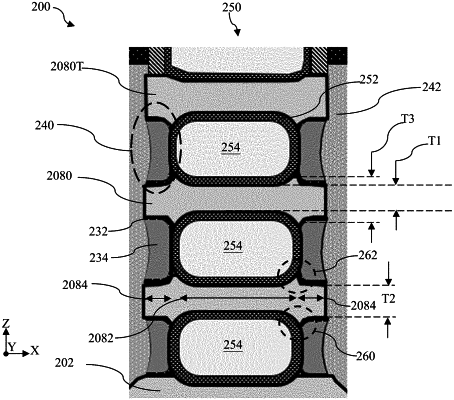
1. A semiconductor structure, comprising:
a nanostructure including a first connection portion, a second connection portion and a channel portion disposed between the first connection portion and the second connection portion;
a first inner spacer feature disposed over and in contact with the first connection portion;
a second inner spacer feature disposed under and in contact with the first connection portion; and
a gate structure wrapping around the channel portion of the nanostructure,
wherein the nanostructure further comprises a first ridge extending upward along a vertical direction from an interface between the channel portion and the first connection portion.
|