| CPC H01L 29/41775 (2013.01) [H01L 21/28114 (2013.01); H01L 21/823468 (2013.01); H01L 21/823475 (2013.01); H01L 29/4175 (2013.01); H01L 29/42376 (2013.01); H01L 29/6653 (2013.01); H01L 29/517 (2013.01)] | 20 Claims |
|
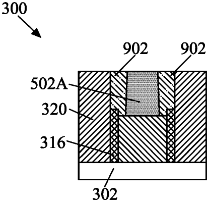
1. A semiconductor device, comprising:
a metal gate structure having sidewall spacers disposed on sidewalls of the metal gate structure;
a metal cap layer disposed over and in contact with the metal gate structure, wherein a first width of a bottom portion of the metal cap layer is greater than a second width of a top portion of the metal cap layer;
a dielectric material disposed on either side of the metal cap layer, wherein the sidewall spacers and a portion of the metal gate structure are disposed beneath the dielectric material; and
an inter-layer dielectric (ILD) layer disposed adjacent to the metal gate structure, wherein a first lateral surface of the ILD layer contacts a second lateral surface of a sidewall spacer that is disposed along a sidewall of the metal gate structure;
wherein a top surface of the metal gate structure and a top surface of the sidewall spacers are both recessed with respect to a top surface of the ILD layer.
|