| CPC H01L 29/41733 (2013.01) [H01L 27/1225 (2013.01); H01L 29/24 (2013.01); H01L 29/45 (2013.01); H01L 29/7869 (2013.01); C22C 29/12 (2013.01)] | 3 Claims |
|
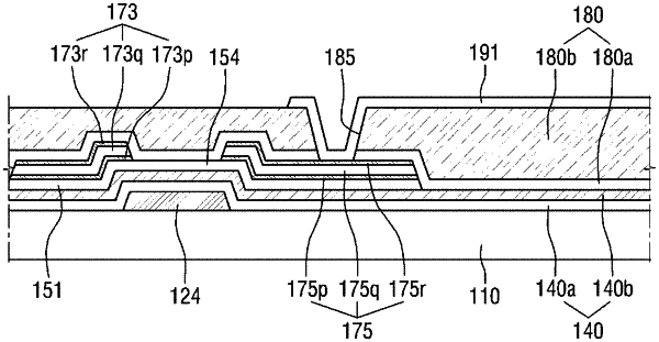
1. A thin film transistor substrate, comprising:
a semiconductor layer; and
source and drain electrodes comprising a metal layer and a barrier layer, the barrier layer interposed between the metal layer and the semiconductor layer and comprising a metal oxide having a crystal size in a c-axis direction between 67 Å and 144 Å,
wherein:
the source and drain electrodes further comprise a capping layer comprising a metal oxide having a crystal size in a c-axis direction between 67.5 Å and 108 Å, the capping layer disposed on the metal layer;
each of the capping layer and the barrier layer comprises one of a bare zinc oxide (ZnO) layer, a gallium-zinc oxide (GZO) layer, an aluminum-zinc oxide (AZO) layer, and an indium-zinc oxide (IZO) layer;
when the capping layer comprises the gallium-zinc oxide (GZO) layer, the gallium-zinc oxide (GZO) layer comprises zinc oxide (ZnO) between 70 weight % and 85 weight % and gallium (Ga) between 15 weight % and 30 weight %,
when the capping layer comprises the aluminum-zinc oxide (AZO) layer, the aluminum-zinc oxide (AZO) layer comprises zinc oxide (ZnO) between 70 weight % and 85 weight % and aluminum (Al) between 15 weight % and 30 weight %, and
when the capping layer comprises the indium-zinc oxide (IZO) layer, the indium-zinc oxide (IZO) layer comprises zinc oxide (ZnO) between 70 weight % and 85 weight % and indium (In) between 15 weight % and 30 weight %.
|