| CPC H01L 27/14623 (2013.01) [H01L 27/14627 (2013.01); H01L 27/14685 (2013.01); H04N 25/70 (2023.01); H01L 27/1464 (2013.01); H01L 27/1469 (2013.01); H01L 27/14634 (2013.01)] | 26 Claims |
|
1. A photoelectric conversion apparatus including a light-receiving region and a light-shielded region, comprising:
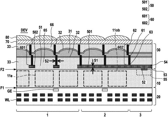
a semiconductor layer in which a plurality of first photoelectric converters are arranged in the light-receiving region and a plurality of second photoelectric converters are arranged in the light-shielded region;
a light-shielding wall arranged above the semiconductor layer and configured to define a plurality of apertures respectively corresponding to the plurality of first photoelectric converters; and
a light-shielding film arranged above the semiconductor layer,
the light-shielding film including a first portion extending along a principal surface of the semiconductor layer to cover the plurality of second photoelectric converters, the first portion having a lower surface on a side of the semiconductor layer and an upper surface on an opposite side of the lower surface, and
the light-shielding wall including a second portion whose distance from the semiconductor layer is larger than a distance between the upper surface and the principal surface,
the light-shielding film defining a plurality of openings corresponding to the plurality of first photoelectric converters, and has a third portion positioned between the second portion and the semiconductor layer,
wherein a thickness of the first portion in a direction perpendicular to the principal surface is larger than a thickness of the second portion in a direction parallel to the principal surface and a thickness of the third portion in the direction perpendicular to the principal surface is larger than a thickness of the second portion in the direction parallel to the principal surface, and
wherein the thickness of the second portion in the direction parallel to the principal surface is defined by the thickest part of the second portion.
|