| CPC H01L 27/1259 (2013.01) [H01L 21/31111 (2013.01); H01L 21/31116 (2013.01); H01L 21/32134 (2013.01); H01L 27/1248 (2013.01); G02F 1/13439 (2013.01); H10K 50/81 (2023.02); H10K 71/621 (2023.02)] | 11 Claims |
|
1. A manufacturing method for a display substrate, comprising:
providing a base;
forming a passivation layer on a surface of the base;
forming an amorphous oxide conductive material layer on a surface of the passivation layer facing away from the base;
forming a photoresist pattern on a surface of the oxide conductive material layer facing away from the base, wherein the photoresist pattern has an exposure region, and a portion of photoresist in the exposure region is removed and a portion of the oxide conductive material layer at a position corresponding to the exposure region is exposed;
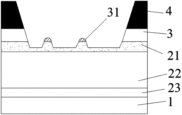
etching the portion of the oxide conductive material layer in the exposure region of the photoresist pattern to form a hollow position exposing a portion of the passivation layer; and
removing a certain thickness material of the portion of the passivation layer exposed through the hollow position,
wherein the passivation layer comprises a first passivation sub-layer and a second passivation sub-layer which are stacked and made of a same material, the second passivation sub-layer is more compact than the first passivation sub-layer, and wherein the first passivation sub-layer is further away from the base than the second passivation sub-layer, and wherein
the removing the certain thickness material of the portion of the passivation layer exposed through the hollow position comprises: removing at least a certain thickness material of a portion of the first passivation sub-layer exposed through the hollow position,
wherein the removing the certain thickness material of the portion of the first passivation sub-layer exposed through the hollow position comprises:
etching a preset depth of the first passivation sub-layer exposed through the hollow position by adopting an anisotropic plasma etching process, and then stopping etching; and
etching the remaining material of the first passivation sub-layer by adopting an isotropic plasma etching process.
|